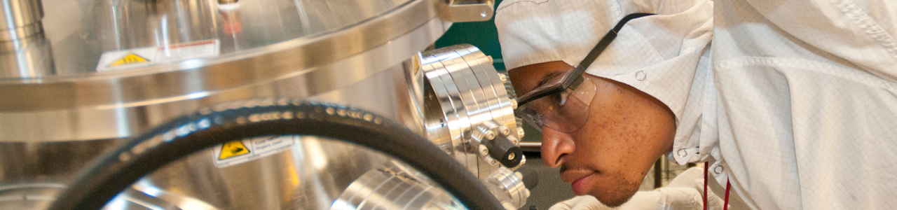
![]() |
|
![]() ![]() ![]() ![]() ![]() ![]() ![]() ![]() ![]() ![]() ![]() ![]() ![]() ![]() ![]() ![]() ![]() ![]() |
![]() |
CNF Lab and Equipment Information
![]() |
![]() |
![]() |
|
|
||||
![]() |
![]() |
![]() |
![]()
Boron Doping - D1
CAC Name: Boron Diffusion Solid Source Boron Diffusion Manager: Phil Infante
Backup: Aaron Windsor
, Daniel McCollister
Equipment Training
Training for the furnace area covers the pre-furnace MOS clean, atmospheric and LPCVD processes. It is scheduled on a need basis, please email the tool manager for training requests. Include MOS area training in the subject header. You will be notified when the next scheduled training will be by email. Description:The Boron Doping Furnace is an atmospheric furnace with a 40” flat zone capable of processing up to 6” diameter wafers. The furnace tube is configured for utilizing solid source wafers for silicon doping. The furnace is restricted to silicon materials. Capabilities:The Boron Doping Furnace is an atmospheric furnace with a 40” flat zone capable of processing up to 6” diameter wafers. The furnace tube is configured for utilizing solid source wafers for silicon doping. The furnace is restricted to silicon materials. Additional Resources:Equipment Information SheetLocation of tool in cleanroom (jpg) Back to Top |
![]() |
![]() ![]() ![]() ![]()
FURNACE PROCESSING
Boron Doping - D1 Carbon Nanotube/Graphene Furnace CMOS N+ Polysilicon - D3 CMOS Wet Oxide - E2 General Material Anneal 1 - A1 LPCVD CMOS Nitride - E4 LPCVD LTO - B3 LPCVD Nitride - B4 MOS Clean Anneal 2 - B1 MOS Clean Hoods MOS Metal Anneal 3 - C1 MOS Metal Anneal 4 - C2 N+/P+ Polysilicon - C4 Phosphorus Doping - D2 TFT LPCVD LTO410 - A3 TFT Polysilicon - A4 TFT Wet/Dry Oxide - A2 Wet/Dry Oxide - B2 Back to Equipment List ![]() |
![]() |
|||
![]() |
![]() ![]() ![]() ![]() |
||
![]() |
![]() This material is based upon work supported by the National Science Foundation under Grant No. ECCS-1542081. Any opinions, findings, conclusions or recommendations expressed in this material are those of the author(s) and do not necessarily reflect the views of the National Science Foundation. Cornell NanoScale Science & Technology Facility (CNF) 250 Duffield Hall, Cornell University, Ithaca, New York 14853-2700 Voice: 607-255-2329, Fax: 607-255-8601, Email: information@cnf.cornell.edu Powered by ITX |